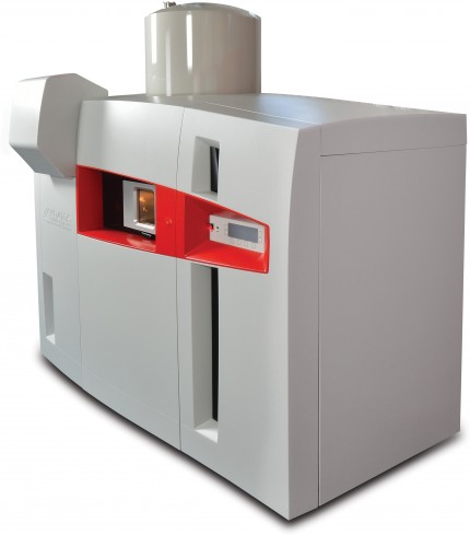
The AXIS Nova combines XPS imaging and spectroscopic capabilities with a highly automated, large sample handling system and is the next generation of AXIS Nova spectrometer. The AXIS Nova is based on Kratos’ proven AXIS technology comprising: magnetic and electrostatic transfer lenses; co-axial electron-only charge neutralisation; spherical mirror and hemispherical electron energy analysers. Kratos developed innovations such as the delay-line detector for spectroscopy and imaging modes and high energy X-ray excitation sources ensure the AXIS Nova is capable of performing in the most demanding research and development environments.

Designed for ease of use, the AXIS Nova has automated sample loading, orthogonal cameras for easy sample positioning and intuitive data acquisition software. A unique capability of the AXIS Nova is the 110mm diameter sample platen allowing unrivalled large sample handling and high sample throughput.
None of these attributes compromise the performance. The AXIS Nova is capable of high sensitivity, excellent energy resolution and fast, high spatial resolution imaging meeting the analysis needs of the most challenging applications.
Capabilities of the AXIS Nova
High Resolution Spectroscopy and Selected Area Spectroscopy
In spectroscopy mode the large radius hemispherical sector analyser (HSA) ensures excellent photoelectron transmission guaranteeing high sensitivity and high energy resolution. Small spot spectroscopy is achieved by inserting an aperture into the electrostatic lens column forming a virtual probe at the surface
This approach to small area analysis removes problems of sample charging and X-ray induced degradation associated with micro-focused X-ray sources. Small spot spectra can be acquired from areas as small as 10µm diameter from any point within the field of view of the lens. A unique electrostatic deflection system allows the position of the virtual probe to be deflected across the surface of the sample. The position for acquisition of small spot spectra can be defined by a simple mouse click from a parallel photoelectron image with the advantage that there is no need for translation of the sample. Alternatively the high resolution in-situ optical microscope image of the sample may be used to define the XPS analysis position directly.
The X-ray source on the AXIS Nova is based on a large 500mm Rowland circle geometry ensuring less energy dispersion in the focused X-ray spot than systems based on smaller Rowland circles. This guarantees the highest energy resolution as demonstrated by a FWHM <0.48eV for Ag 3d. The Al Kα X-rays are monochromated by a single toroidal backplane for ease of alignment of the X-ray spot with the analysis position. The X-ray anode is engineered to allow indexed movement of the anode surface with respect to the cathode. Thus new anode surface may be exposed as required without breaking vacuum. The availability of 10 anode positions significantly increases the useful lifetime of the anode.
Quantitative Parallel Imaging
The AXIS Nova provides unrivalled performance for fast elemental and chemical state imaging. The spectrometer uses a 165mm mean radius hemispherical analyser (HSA) for spectroscopy combined with the Kratos patented spherical mirror analyser (SMA) for parallel imaging.
In parallel imaging mode photoelectrons at a discrete kinetic energy (binding energy) are focused on the two-dimensional photoelectron detector producing a direct image of the surface without scanning. The relative position of the photoelectrons is maintained as they pass through the SMA allowing acquisition of parallel images in a matter of seconds in contrast to the slower pixel by pixel acquisition of XPS mapping. The speed of parallel image acquisition has the obvious advantage of reducing X-ray exposure to delicate samples. Using a 256 x 256 pixel array, parallel XPS images of the sample surface with a spatial resolution of <3µm can be acquired. Elemental or chemical differences may be easily imaged even if they are not visible by optical inspection. The properties and design of the SMA mean that the parallel images have both high spatial and high energy resolution. Data (below) show hydrocarbon and C-F chemical state images for a plasma patterned sample. images may also used to define the analysis position for small spot selected are spectra without translating the sample.
Charge Neutralisation
The AXIS Nova charge neutraliser is based upon proven market leading technology used in over 250 AXIS spectrometers. The use of a coaxial low energy electron source within the field of the magnetic lens ensures that the ultimate base pressure of the spectrometer is maintained during analysis of insulating samples in contrast to other neutralisation systems which require an additional source of Ar+ ions. The advanced design of the Kratos neutraliser ensures that the system is self-regulating and works effectively on all classes of insulating materials including fibres, powders and thin films. When used in conjunction with the monochromatic X-ray source, spectra with unrivalled energy resolution may be generated from electrically insulating materials as demonstrated by data showing FWHM of <0.68eV on the ester component in polyethylene terephthalate (PET).
Large Sample Handling
The AXIS Nova sample handling and platen navigation system integrates in-situ optical microscopes with the acquisition software for easy, rapid definition of sample analysis positions. Both full platen (110mm diameter field of view) and high magnification (2mm field of view) high resolution optical images can be saved into a dataset and recalled for sample positioning. A large view port allows the user to see the platen in the analysis chamber giving complete confidence in sample location.
Delay-Line Detector
Kratos Analytical continues to lead in the development of imaging X-ray photoelectron spectrometers with the introduction of the delay-line detector (DLD). Representing the next generation of photoelectron detectors, the DLD provides a single pulse counting detector for both spectroscopy and imaging experiments. Comprising a multi-channel plate stack above two orthogonal delay-line anodes and associated electronic control units, the DLD is at the heart of the AXIS Nova. With a large active area the DLD possesses 128 channels for photoelectron detection in spectroscopy mode. The high number of channels means that, as well as collecting photoelectrons in usual energy scanning mode, the spectrometer can also be used to collect spectra with 128 data points without scanning the analyser, also known as ‘snapshot’ spectroscopy. This mode allows an individual photoelectron peak to be collected in less than 1 second with obvious advantages for data acquisition during depth profiling or dynamic surface characterisations.
When used in parallel imaging mode photoelectrons with 2D spatial distribution are incident on the DLD. The fast DLD control electronics convert the electron arrival position on each of the two delay-line anodes into an x, y co-ordinate for every electron event. Integrating the signals over several seconds allows the generation of truly quantitative elemental or chemical images of the surface over a 65,500 pixel array. In the highest magnification imaging mode the spatial resolution at the surface is <3µm. A significant advantage of the digital DLD technology is that the system has inherent low noise characteristics with spike immunity assured.


