EBIC acquisition

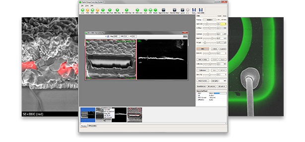
The best quantitative electronics and software for Electron Beam Induced Current(EBIC)
Make the link between device characterization and materials properties
- Image electrical activity across complete devices
- Distinguish between electrically active and passive defects
- Correlate electrical activity with composition (EDS) and crystallographic structure (EBSD)
Localise electrical defects with highest resolution
- Enable sample preparation for TEM or atom probe microscopy
- Avoid alignment errors by directly imaging defects with EBIC in FIB SEM
- Use live EBIC imaging to stop milling during sample preparation
Map junctions and defects over large areas
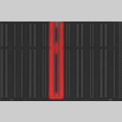
- Identify all electrically active defects
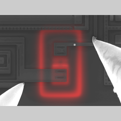
- Map active areas of junctions and electrical fields
- Validate doping profiles and areas
Export calibrated EBIC signal for analysis of materials properties
- Measure defect contrast / recombination strength
- Extract diffusion length of minority charge carriers
- Determine width of depletion regions
Verify device operation modes with built-in biasing and live overlay
- Image junctions and fields in delayered devices
- Map electrical activity in solar cells under bias
- Compare imaged behaviour with device modelling
Access third dimension with depth profiling
- Manipulate depth of EBIC signal by changing kV in SEM
- Investigate EBIC images of cross-sections in FIB-SEM
- Export EBIC depth series for 3D reconstruction
Pictures/Videos

